The Ultimate Guide to Xilinx Training
Xilinx FPGA Design

Quick view
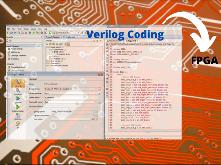
"Verilog & FPGA Design - 6 Days Comprehensive course"
What you'll learn :
- Comprises of 2 course modules Designing with Verilog and Essentials of FPGA. Comprehensive course is a through Introduction to the Verilog Language.
- Emphasis is on writing Register Transfer Level (RTL) and behavioral source code.
- This class addresses targeting targeting Xilinx devices specifically and FPGA devices in general.
- How to applied to any digital design by using a top-down synthesis design approach?.
- Learn advanced coding techniques that will increase your overall proficiency and enhance FPGA Optimization.
- The ability to write efficient hardware designs and perform high level HDL-Simulations.
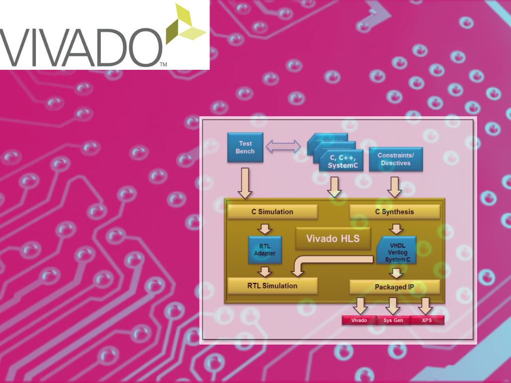
- Build and effective FPGA design using synchronous design techniques, instantiate appropriate device resources, use proper HDL coding techniques, make good pin assignments, set basic XDC timing constraints, and use the Vivado® Design Suite to build, synthesize, implement, and download a design.
- Hands-On Project (1 day) that allows you to test your knowledge and apply your skills immediately
Enquire Now!!
Complete the form to get a quotation and consult with our sales representative.
COURSE DETAILS
Course Objective
This course offers 6 days comprehensive training package that comprises 2 modules Designing with Verilog and Essentials of FPPGA. The emphasis is on writing Register Transfer Level (RTL) and behavioral source code. This class addresses targeting Xilinx devices specifically and FPGA devices in general. Offering 1 days hands-on project to test knowledge and apply skills immiditely.
Who should attend
Digital designers who are interested in FPGA design training and want to use Verilog effectively for modeling, design, and synthesis of digital designs and learn to use Xilinx FPGAs.
DURATION
6 days
Module 1: Designing with Verilog
Day 1
1.1 Introduction to Verilog
1.2 Verilog Keywords and Identifiers
1.3 Verilog Data Types
1.4 Verilog Buses and Arrays
1.5 Verilog Modules and Ports
1.6 Demo: Multiplexer
1.7 Lab 1: Building Hierarchy
1.8 Verilog Operators
1.9 Continuous Assignment
1.10 Gate-Level Modeling
1.11 Procedural Assignment
1.12 Blocking and Non-Blocking Procedural Assignment
1.13 Lab 2: Creating a Simple Memory
1.14 Procedural Timing Control
Day 2
1.1 Introduction to Verilog
1.2 Verilog Keywords and Identifiers
1.3 Verilog Data Types
1.4 Verilog Buses and Arrays
1.5 Verilog Modules and Ports
1.6 Demo: Multiplexer
1.7 Lab 1: Building Hierarchy
1.8 Verilog Operators
1.9 Continuous Assignment
1.10 Gate-Level Modeling
1.11 Procedural Assignment
1.12 Blocking and Non-Blocking Procedural Assignment
1.13 Lab 2: Creating a Simple Memory
1.14 Procedural Timing Control
Day 3
3.1 Verilog Timing Checks
3.2 Finite State Machine
3.3 Finite State Machine: Mealy
3.4 Lab 6: Building a Mealy Finite State Machine
3.5 Finite State Machine: Moore
3.6 Lab 7: Building a Moore Finite State Machine
3.7 FSM Coding Guidelines
3.8 File I/O Introduction
3.9 File I/O Read Functions
3.10 Lab 8: Using Verilog File I/O
3.11 File I/O Write Functions
3.12 Targeting Xilinx FPGAs
3.13 Lab 9: Implementing and Downloading the Design
3.14 User-Defined Primitives
3.15 Programming Language Interface
Module 2: FPGA Design Expert
Day 4
- Design Methodology Summary
- Basic FPGA Architecture
- Vivado IDE Features and Benefits
- Introduction to the Vivado Design Suite
- Vivado IDE Project Manager and IP Library
- Vivado IDE Tool Overview
- Lab 1: Vivado Tool Overview
- Vivado IDE Synthesis and Report
- Vivado IDE Implementation and Static Timing Analysis
- Lab 2: Vivado Synthesis and Implementation
Day 5
- Designing with FPGA Resources
- Clocking Resources
- Lab 3a: Designing with FPGA Resources
- Lab 3b: Creating an IP Integrator Subsystem Design
- Basic Timing Constraints (XDC)
- Timing Reports
- Lab 4: Basic XDC and Timing Reports
- Synchronous Design Techniques
- FPGA Configuration
- Appendix: SystemVerilog
- Appendix: Design Methodology
- Appendix: HDL Coding Techniques
Day 6
- Full FPGA Design Flow Hands-on Project
Find the right Xilinx course for you
Xilinx FPGA Design
FPGA Design Expert
‘This course offers introductory training on the Vivado® Design Suite and demonstrates the FPGA design flow for those uninitiated to FPGA design. Read more>>
Xilinx FPGA Design
Accelerating Applications with the Vitis Unified Software Environment
Learn how to develop, debug, and profile new or existing C/C++ and RTL applications in the Vitis™ unified software environment targeting both data center (DC) and embedded applications. Also learn how to run designs on the Xilinx Alveo™ accelerator card using Nimbix Cloud.
Xilinx SOC and MPSOC
Zynq UltraScale+ MPSoC for the System Architect
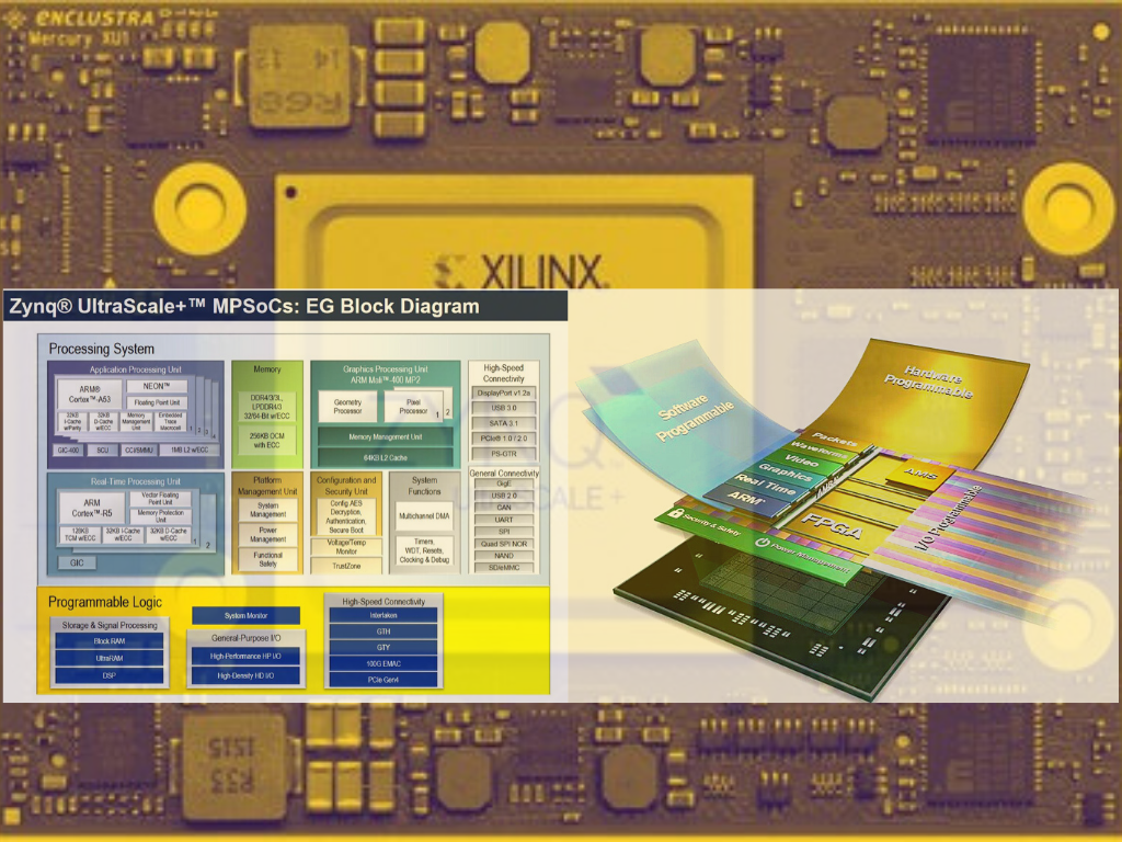
Zynq® UltraScale+™ MPSoC devices provide 64-bit processor scalability while combining real-time control with soft and hard engines for graphics, video, waveform, and packet processing. Built on a common real-time processor and programmable logic equipped platform, three distinct variants include dual application processor (CG) devices, quad application processor and GPU (EG) devices, and video codec (EV) devices, creating unlimited possibilities for applications such as 5G Wireless, next generation ADAS, and Industrial Internet-of-Things. Read more>>
Xilinx Vivado / FPGA Design
Advanced Timing Closure Techniques for the Vivado Design Suite
Achieving repeatable and reliable timing is the designer’s ultimate goal. The task of writing timing constraints and validating the design against those constraints is commonly referred to as Timing Closure. This process is essential for every design. This course will provide experienced Vivado® Design Suite users with the skills to ensure that their designs work reliably over process, voltage, and temperature variations.


